Company tel:+86-379-63184520
Contact number:+86-15937921751
Postcode:471000
Email:info@yuxindiamond.com
Address:3-1-508 Luoyang National University Science Park, No. 2 Penglai Road, Jianxi District, Luoyang, China 471000
On-chip Excitation of Nanodiamonds Embedded in Plasmonic Waveguides
Quantum emitters can be integrated in monolithic nanoscale plasmonic circuitry via low-loss plasmonic configurations to confine light well below the diffraction limit. In integrated quantum plasmonics, waveguides based on surface plasmon polariton (SPP) modes that propagate electromagnetic waves along metal-dielectric or metal-air interfaces are superior to dielectric-based (and therefore diffraction-limited) photonic waveguides. The observation is in respect to the available Purcell enhancement from embedded quantum emitters and the ongoing trend toward on-chip integration and miniaturization to realize optical signal processing and integrated circuits. Different metal-dielectric configurations have been developed for strong light-matter interactions at the scale of the single photon to support the propagation of plasmonic modes confined beyond the diffraction limit. The property can enable unique prospects to design highly integrated photonic-signal processing systems, sensors and optical imaging techniques with nanoscale resolution.
A variety of SPP-based structures created in the past include metal nanowires (NW), parallel NWs, V-grooves (VGs) and wedge waveguides that have demonstrated single plasmon guidance for potential quantum applications. The practical realization of such integrated quantum photonics has remained elusive due to several challenges, including high propagation losses of SPP modes and the limited control on single quantum emitters. More recently, studies have nanofabricated low-loss, dielectric-loaded SPP waveguides (DLSPPWs) structured on a silver film for simple quantum plasmonic circuits composed of embedded nanodiamonds with nitrogen-vacancy centers.
Hamidreza Siampour and co-workers have taken a step forward in the field of integrated quantum plasmonics by demonstrating on-chip coupling between a single photon source and plasmonic waveguide. In the approach, the physicists engineered a nanodiamond featuring a germanium vacancy (GeV) center that emits single photons, embedded inside a plasmonic waveguide composed of dielectric hydrogen silsesquioxane (HSQ) atop a layer of silver fabricated using electron-beam lithography. When a green laser light (532 nm) was coupled to one end of the waveguide via grating couplers to propagate to the nanodiamond, it excited the GeV center, which emitted a single photon that coupled into the plasmon mode of the waveguide. In the work, the researchers achieved long waveguide transmission lengths (33 µm) and efficient coupling (56 percent) to open new avenues in the development of chip-based quantum circuitry.
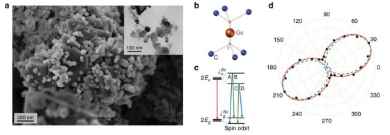
The study was the first to detail the synthesis and characterization of the GeV nanodiamonds. The nanodiamonds were produced using the high-pressure, high-temperature (HPHT) method; Ge was introduced during the growth process to incorporate single GeV centers. The scientists proposed and demonstrated a hybrid approach for nanofabrication using DLSPPW structured on single silver (Ag) crystals that considerably lowered SPP dampening rates, compared to Ag films fabricated by other techniques. The method facilitated sufficiently long SPP propagation at the excitation and emission wavelengths of GeV centers in nanodiamonds incorporated within a plasmonic chip.
The structure of the synthetic GeV nano and microdiamonds were observed in the raw sample using scanning electron microscopy (SEM) and transmission electron microscopy (TEM). Synthetic nanodiamonds were spin coated onto Ag-coated silicon wafers and scanned with confocal fluorescence microscopy. Measured data indicated ultrabright, spectrally narrow and stable single photon sources based on single GeV centers in the nanodiamonds, suitable for highly integrated circuits. The polarization characteristics of the GeV nanodiamonds were measured using an analyzer in the detection pathway to determine the projection of single photons emitted on the surface plane. The data measured for a single GeV nanodiamond fit the model polarization characteristics of diamond color centers based on group-IV elements in the periodic table (e.g. silicon-vacancy SiV, germanium-vacancy GeV, and tin-vacancy SnV).
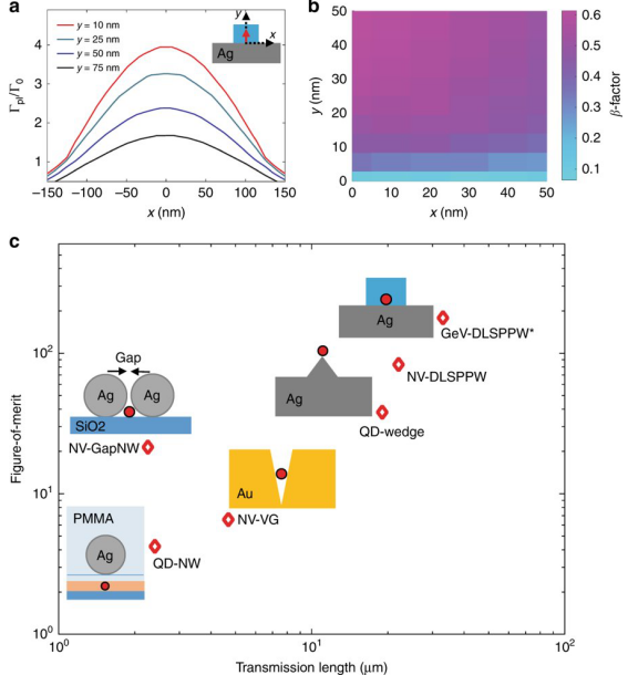
The observed capacity for single-photon emission in diamond nanocrystals can enable hybrid quantum-plasmonic systems that can facilitate remote excitation of the GeV centers incorporated in a plasmonic chip. Siampour et al. elegantly demonstrated the efficient long-range delivery of the GeV-DLSPPW system compared with other hybrid quantum plasmonic systems. An exceptional figure of merit (FOM) of 180 was revealed in the study due to a ~six-fold Purcell enhancement, 56 percent coupling efficiency and ~33 µm transmission length at a wavelength (λ) of 602 nm.
Electron beam lithography was used to fabricate the waveguides with HSQ resist on Ag-coated substrates to contain the nanodiamonds featuring single GeV centers - added via controlled placement into the device. The technology provided ~30 nm precision in placement, enhanced via observations with SEM imaging, limited by the size of nanodiamonds, which could be fabricated down to 1 nm using existing diamond synthetic technology. The fabricated waveguide was visualized with atomic force microscopy (AFM) and with a charge coupled device (CCD) camera after nanodiamond excitation via a green pump laser.

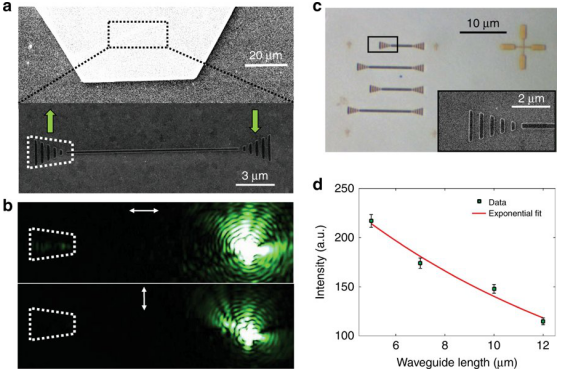
Additionally, the authors used a single crystalline Ag flake instead of Ag film to significantly enhance the DLSPPW propagation length. Green laser light transmitting through the DLSPPW mode was optically characterized as polarization along the waveguide axis. Transmission was measured for several waveguides of varying lengths to show extraordinary propagation lengths (~11.8 µm) for the green laser light through the low-loss DLSPPW.
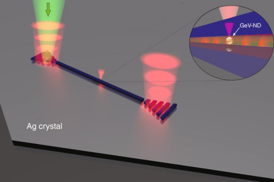
Using a similar set-up, the scientists proceeded to demonstrate and confirm remote excitation of the GeV center coupled to the DLSPPW mode. Subsequently, the GeV decay rate was simulated using the finite element modeling (FEM) method and a decay rate of up to four-fold was predicted for a GeV center in the waveguide compared to its emission in vacuum. The system demonstrated superior performance when compared with previously demonstrated systems, the observed Purcell factor can be further enhanced in future studies by using a larger refractive index dielectric such as titanium dioxide (TiO2).
The study opens the way to integrate an excitation laser, quantum emitter and plasmonic circuit onto the same chip. Previous strategies have demonstrated the detection of single plasmons and two-plasmon interference on a chip. By combining all three technologies on a single chip, the authors envision that it will be possible to integrate all elements of a quantum plasmonic circuit on a chip in the near future.
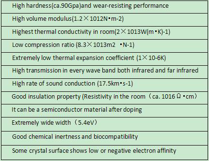
Diamond, as one of the most special materials in natural world, is featured with the highest hardness, low friction coefficient, high elasticity modulus, high thermal conductivity, high insulation class, wide energy gap, great sound propagation rate and favorable chemical stability, which are presented in below Table. In spite of such unique features, the natural diamond has always been existed in the form of gem, with its variability and rareness sharply limiting its application. Luoyang Yuxin Diamond Co., Ltd‘s CVD Diamond film, on the other hand, integrates such physical and chemical properties, with lower cost than natural diamond and applicable to be made into various shapes, thus enjoying extensive application prospect in electronic industry, optical field and mechanical industry.
