Company tel:+86-379-63184520
Contact number:+86-15937921751
Postcode:471000
Email:info@yuxindiamond.com
Address:3-1-508 Luoyang National University Science Park, No. 2 Penglai Road, Jianxi District, Luoyang, China 471000
Nanodiamond-based Controllable Light Source
hysicists from ITMO University and Australian National University have developed the first-ever controlled nanodiamond-based light source. Experiments have shown that diamond shells can double the emission speed of light sources and help control them without any additional nano- and microstructures. This result was achieved due to artificially created defects in the diamonds’ crystal lattice. Results of this research are important for the development of quantum computers and optical networks.
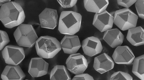
One of the key areas of modern nanophotonics is the design of active dielectric nanoantennas or controlled photonic sources. As a base for nanoantennas, scientists usually use plasmonic metal nanoparticles. However, optical loss and heating of these particles encourages scientists to look for alternatives. For example, ITMO University researchers created nanoantennas based on perovskites and silicon. Recently, members of the International Laboratory for Nanophotonics and metamaterials of ITMO University developed a new concept of active dielectric nanoantennas based on nanodiamonds.
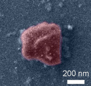
Nanodiamonds are carbon nanostructures with unique properties. They have a sufficiently high refractive index, high thermal conductivity, and low interaction activity. The scientists used nanodiamonds with so-called nitrogen-vacancy centers (NV-centers). These are created artificially by removing carbon atoms from a diamond’s crystal lattice. The opened vacancy is then linked to an implanted nitrogen atom. The electron spin of such NV-centers is easily controlled by light, and that electron spin can be used to record quantum information.
Scientists from ITMO University studied the optical properties of nanodiamonds and found that their radiation can be enhanced by combining the NV-center luminescence spectrum with optical Mie resonances of diamond nanoparticles. This can be achieved at a certain position of the NV-center and the appropriate particle size. This way one can increase the nanodiamond’s Purcell factor. This indicator is used to estimate how a diamond shell affects the rate of spontaneous emission of the light source. If the Purcell factor increases, the luminescence fade time reduces while the signal itself becomes stronger and much easier to read.
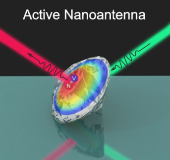
The researchers emphasize that this effect is achieved by using only properties of nanodiamonds. "Usually, to accelerate the radiation, one has to create a complex system of resonators. But we managed to achieve similar results without any additional structures. We showed experimentally that the luminescence fading can be speeded up at least two times, using just simple physics," says Dmitry Zuev from The International Laboratory for Nanophotonics and Metamaterials.
In fact, experiments were carried out on nanodiamonds with multiple NV-centers, even though the researchers also developed a theoretical model for the behavior of single photon sources in the diamond shell. Calculations showed that the speed of light emission can be increased by several dozen times.
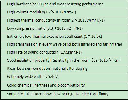
Diamond, as one of the most special materials in natural world, is featured with the highest hardness, low friction coefficient, high elasticity modulus, high thermal conductivity, high insulation class, wide energy gap, great sound propagation rate and favorable chemical stability, which are presented in below Table. In spite of such unique features, the natural diamond has always been existed in the form of gem, with its variability and rareness sharply limiting its application. Luoyang Yuxin Diamond Co., Ltd‘s CVD Diamond film, on the other hand, integrates such physical and chemical properties, with lower cost than natural diamond and applicable to be made into various shapes, thus enjoying extensive application prospect in electronic industry, optical field and mechanical industry.
