Company tel:+86-379-63184520
Contact number:+86-15937921751
Postcode:471000
Email:info@yuxindiamond.com
Address:3-1-508 Luoyang National University Science Park, No. 2 Penglai Road, Jianxi District, Luoyang, China 471000
Applied to EUV lithography in CVD diamond infrared optics
The infrared (IR) transmission substrate based on the plasma EUV lithography source must face a strict optical and physical environment, combined with high infrared transmission, strength, and stability. Whereas CVD diamond is qualified for this role.
Diamond has long been known as having excellent properties, largely due to the symmetry of cubic lattice making the carbon atoms very strong. Thanks to its high hardness, it has been primarily used in mechanical applications. However, its thermal and semiconductor properties are also used in sensors. As early as 1978, diamonds were used for optics. For example, Due to the transparent width of the diamond substrate as well as the excellent mechanical properties, the diamond is used for the Pioneer Venus orbiter of the spacecraft and the wide substrate of the infrared (IR) spectrometer. However, natural diamonds are generally not available in optically necessary dimensions and can not meet the quality requirements of engineering solutions. The second key feature of diamond is its high breaking strength, especially when optics are used as a partition between a large number of different pressures. A typical diamond substrate design effectively maintains the pressure, which is four times more than that of a substrate made of zinc sulfide. This higher breaking strength significantly reduces the overall absorbance in the system. The third important parameter is the thermal conductivity at room temperature where the diamond has the highest compared to other solids, above 2000 W / mk. For optical engineers, diamond with low coefficient of thermal expansion is very useful. Even when the diamond substrate is heated, the low CTE ensures that the substrate does not significantly change the shape and minimizes the thermal lens effect. Compared to other materials, CVD diamond has greatly improves the beam quality .
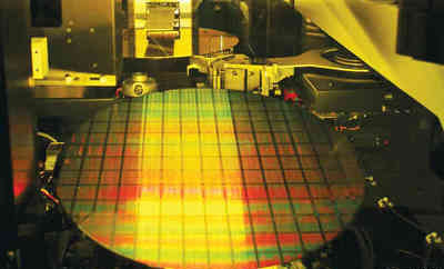
Optical grade diamond is the only material that can make EUV lithography technology which is of high input power to improve system throughput.
Our company, Luoyang Yuxin Diamond Co., Ltd., produces CVD (Chemical Vapor Deposition) diamond film is made by chemical vapor deposition process. It is in transparent after being double-sided polished. The regular diameter can be up to more than 120 mm, and its light transmittance can be up to more than 60% when its thickness is 1 mm. As the typical multifunctional material, the diamond provides high thermal conductivity, high refractive index, radiation resistance, chemical inertness, excellent electrical and mechanical properties, and it is particularly suitable for infrared optical window with 8~12μm long wave.
In all the infrared optical materials, CVD diamond film is the only material combining light transmission, thermal shock resistance and with high durability to the impact of raindrops and solid particles as well as chemical corrosion. More importantly, the extremely low thermal expansion coefficient and high thermal conductivity makes the diamond with excellent ret resistance. It keeps nice optical performance in high temperature environment, making it the best material for infrared optical windows serving in harsh environment. Our products are widely applied in window materials for high power laser and detector, protective film for optical lens, radiation detectors and missile radome, etc.
Contact number:+86-15937921751 Company tel:+86-379-63184520
Postcode:471000 Email:info@yuxindiamond.com
Address:3-1-508 Luoyang National University Science Park, No. 2 Penglai Road, Jianxi District, Luoyang, China 471000
Copyright:Luoyang Yuxin diamond Co., Ltd.