Company tel:+86-379-63184520
Contact number:+86-15937921751
Postcode:471000
Email:info@yuxindiamond.com
Address:3-1-508 Luoyang National University Science Park, No. 2 Penglai Road, Jianxi District, Luoyang, China 471000
Deep-depletion: A New Concept for Diamond MOSFETs
Diamond is largely recognized as the most ideal material in WBG development, owing to its superior physical properties, which allow devices to operate at much higher temperatures, voltages and frequencies, with reduced semiconductor losses.
A main challenge, however, in realizing the full potential of diamond in an important type of FET—namely, metal-oxide-semiconductor field-effect transistors (MOSFETs)—is the ability to increase the hole channel carrier mobility. This mobility, related to the ease with which current flows, is essential for the on-state current of MOSFETs.
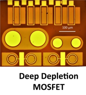
Researchers from France, the United Kingdom and Japan incorporate a new approach to solve this problem by using the deep-depletion regime of bulk-boron-doped diamond MOSFETs. The new proof of concept enables the production of simple diamond MOSFET structures from single boron-doped epilayer stacks. This new method, specific to WBG semiconductors, increases the mobility by an order of magnitude. The results are published this week in Applied Physics Letters.
In a typical MOSFET structure, an oxide layer and then a metal gate are formed on top of a semiconductor, which in this case is diamond. By applying a voltage to the metal gate, the carrier density, and hence the conductivity, of the diamond region just under the gate, the channel, can be changed dramatically. The ability to use this electric "field-effect" to control the channel conductivity and switch MOSFETS from conducting (on-state) to highly insulating (off-state) drives their use in power control applications. Many of the diamond MOSFETs demonstrated to date rely on a hydrogen-terminated diamond surface to transfer positively charged carriers, known as holes, into the channel. More recently, operation of oxygen terminated diamond MOS structures in an inversion regime, similar to the common mode of operation of silicon MOSFETS, has been demonstrated. The on-state current of a MOSFET is strongly dependent on the channel mobility and in many of these MOSFET designs, the mobility is sensitive to roughness and defect states at the oxide diamond interface where unwanted carrier scattering occurs.
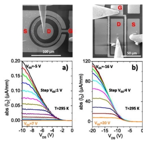
To address this issue, the researchers explored a different mode of operation, the deep-depletion concept. To build their MOSFET, the researchers deposited a layer of aluminum oxide (Al2O3) at 380 degrees Celsius over an oxygen-terminated thick diamond epitaxial layer. They created holes in the diamond layer by incorporating boron atoms into the layer. Boron has one less valence electron than carbon, so including it leaves a missing electron which acts like the addition of a positive charge, or hole. The bulk epilayer functioned as a thick conducting hole channel. The transistor was switched from the on-state to the off-state by application of a voltage which repelled and depleted the holes—the deep depletion region. In silicon-based transistors, this voltage would have also resulted in formation of an inversion layer and the transistor would not have turned off. The authors were able to demonstrate that the unique properties of diamond, and in particular the large band gap, suppressed formation of the inversion layer allowing operation in the deep depletion regime.
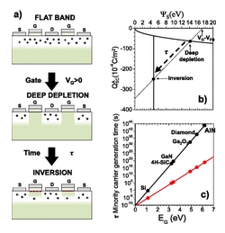
"We fabricated a transistor in which the on-state is ensured by the bulk channel conduction through the boron-doped diamond epilayer," said Julien Pernot, a researcher at the NEEL Institute in France and an author of the paper. "The off-state is ensured by the thick insulating layer induced by the deep-depletion regime. Our proof of concept paves the way in fully exploiting the potential of diamond for MOSFET applications." The researchers plan to produce these structures through their new startup called DiamFab.
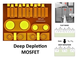
Pernot observed that similar principles of this work could apply to other WBG semiconductors. "Boron is the doping solution for diamond," Pernot said, "but other dopant impurities would likely be suitable to enable other wide bandgap semiconductors to reach a stable deep-depletion regime."
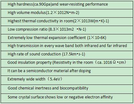
Diamond, as one of the most special materials in natural world, is featured with the highest hardness, low friction coefficient, high elasticity modulus, high thermal conductivity, high insulation class, wide energy gap, great sound propagation rate and favorable chemical stability, which are presented in below Table. In spite of such unique features, the natural diamond has always been existed in the form of gem, with its variability and rareness sharply limiting its application. Luoyang Yuxin Diamond Co., Ltd’ s CVD Diamond film, on the other hand, integrates such physical and chemical properties, with lower cost than natural diamond and applicable to be made into various shapes, thus enjoying extensive application prospect in electronic industry, optical field and mechanical industry.
