Company tel:+86-379-63184520
Contact number:+86-15937921751
Postcode:471000
Email:info@yuxindiamond.com
Address:3-1-508 Luoyang National University Science Park, No. 2 Penglai Road, Jianxi District, Luoyang, China 471000
Higher Performance Semiconductor Technology——Diamond
Diamond has many advantages such as faster speed, lower power consumption, lighter weight and thinner thickness than silicon, which has a great prospect in the semiconductor field.
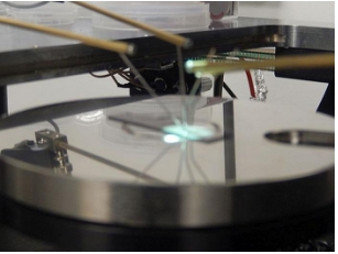
As early as 2000, Argonne National Laboratory have already started tests on chemical vapor deposition (CVD) diamond, and set up Advanced Diamond Technology company. The company has partnered with Innovative Micro Technology to create a diamond MEMS and to promote the CVD equipment used by diamond wafer specialty companies such as SP3 Diamond Technology to deposit diamond crystals. Although the biggest applications for diamonds so far have been in the areas of jewelery, abrasives and artificial diamonds, Argonne National is still struggling to find ways to make diamonds (natural insulators) into semiconductors and conductors, Diamond chips pave the way. Akhan Semiconductor, a US startup, has been licensed by the U.S. Department of Energy's Argonne National Laboratory for Diamond Semiconductor Process technology and is planning to be the first to truly bring its semiconductor products to market, in conjunction with its technological breakthrough in the diamond area.
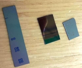
The biggest problem with commercializing the diamond semiconductor is making P-type transistors easily and making n-type transistors difficultly. Adam Kahn, founder and CEO of Akhan Semiconductor, offers the "Miraj Diamond Platform" as a solution that makes P-type and N-type Type device possible to manufacture a diamond complementary metal oxide semiconductor (CMOS). The technological core of the process platform is that by doping phosphorus in a P-type device, it is doped with barium and lithium in the N-type device, resulting in tunable electronic devices with comparable P-type and N-type performance, and thus the result is diamonds CMOS.
Akhan Semiconductor's first device manufactured using a CMOS-based diamond semiconductor process is a diamond PIN diode with a thickness record-breaking of 500 nanometers, one million times better performance than silicon and 100 times thinner than silicon, due to the band gap ratio is even wider silicon carbide and gallium nitride; in thermal analysis, there is no hot spot in the PIN diode, so there is no parasitic loss in the silicon PIN diode.

Akhan Semiconductor also showed 100GHz devices. The ultra-low resistance of diamond to reduce thermal requirements, as well as deposition on silicon, glass, sapphire and metal substrates, is expected to revive the evolution of microprocessor operation. Previously, due to the inability to effectively dissipate heat, the computing speed of microprocessors has been hovering for 10 years at about 5 GHz. For silicon, 5GHz is a limit result from higher power consumption and hot spots turn microprocessors into bubbles, while diamonds have 22 times the thermal conductivity of silicon and 5 times the thermal conductivity of copper, Reach a new height, spawned a new generation of microprocessors. Diamond technology will also continue Moore's Law. The 100GHz chip exhibited by Akhan Semiconductor uses a feature size of 100s nanometers, with 12 generations before the diamond faces a single atomic level, while silicon will reach its atomic-growth limit by 2025.
Akhan company's products will be the future’ s core components of smart phones, smart watches, laptop or virtual reality glasses. Akhan's products not only improve the performance of the equipment, but also increase the life of the equipment. why? The answer is simple: diamonds. More precisely: synthetic diamonds.

Diamonds are not only the hardest material on the Mohs scale, but also with good thermal conductivity. Diamonds are more energy-conserving than silicon. For smartphones, diamond-based processors reduce the amount of heat generated.
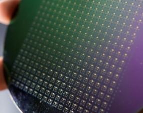
Smartphones are not the only beneficiaries, and diamond processors can help those who want to reduce the size of their circuits in the device. In addition, heavy industry and the aerospace industry also require diamond-processing devices to withstand high levels of radiation and X-rays.
November 15th, AKHAN Semiconductor announced that the issuance by the Japan Patent Office of a patent covering a method for the fabrication of diamond semiconductor materials, core to applications in automotive, aerospace, consumer electronics, military, defense, and telecommunications systems, amongst others.
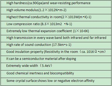
Diamond, as one of the most special materials in natural world, is featured with the highest hardness, low friction coefficient, high elasticity modulus, high thermal conductivity, high insulation class, wide energy gap, great sound propagation rate and favorable chemical stability, which are presented in below Table. In spite of such unique features, the natural diamond has always been existed in the form of gem, with its variability and rareness sharply limiting its application. Luoyang Yuxin Diamond Co., Ltd’ s CVD Diamond film, on the other hand, integrates such physical and chemical properties, with lower cost than natural diamond and applicable to be made into various shapes, thus enjoying extensive application prospect in electronic industry, optical field and mechanical industry.
