Company tel:+86-379-63184520
Contact number:+86-15937921751
Postcode:471000
Email:info@yuxindiamond.com
Address:3-1-508 Luoyang National University Science Park, No. 2 Penglai Road, Jianxi District, Luoyang, China 471000
Diamond-based Sensors Enable Spintronics and Next-generation MRI

Sensors developed under the DIADEMS project and capable of measuring magnetic fields with unprecedented accuracy are on the path to commercialisation. The technology has already spurred the creation of four start-ups.
The DIADEMS project has come a long way since it was covered by CORDIS in 2016. At the time, the consortium aimed to use artificial diamonds to sense magnetic fields down to the nanometre. Now completed, DIADEMS exceeded all expectations, and market applications – along with a potential new project – are on their way.
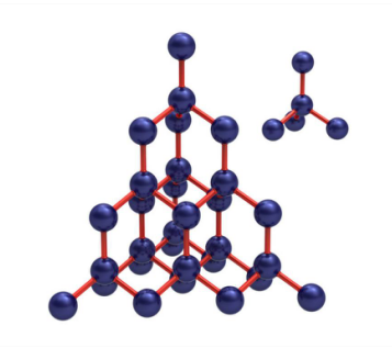
DIADEMS' sensors are based on "nitrogen-vacancy" (NV) colour centres in ultra-pure artificial diamonds: A single carbon atom in an ultrapure single crystal diamond is replaced with a nitrogen atom, and the neighbouring lattice site void creates a Nitrogen Vacancy centre (NV). This, in turn, enables the development of atomic-scale magnetometers with very high sensitivity for various applications.
"One of these applications is a wide field magnetic imager for monitoring electronic circuits. This is a new tool that is very convenient to use since it works at room temperature and in ambient atmospheric conditions," says Thierry Debuisschert, coordinator of DIADEMS for Thales Research & Technology.
"Other applications include the experimental characterisation of read/write heads for high density hard disks to increase their capacity; nuclear magnetic resonance (NMR) boasting higher sensitivity, lower cost and a reduced magnetic field in MRI machines; new photonic devices increasing the detection efficiency of NV fluorescence; a spectrum analyser for the GHz range and the characterisation of domains in antiferromagnetic materials."
With all that potential, it's no surprise to see side-projects sprouting across Europe. Project Partner Attocube Systems, for instance, is currently developing a combination of an atomic force and a confocal microscope using a single NV centre as a sensor, for commercial use. Element 6, another project partner, has already enriched its portfolio with advanced materials based on NV centres. "A total of four start-ups have also been launched by project partners: NVision, SQUTEC, QNAMI and QZABRE," explains Debuisschert.
"We have been very active since the end of the project," he adds. "We aim for higher bandwidth, sensitivity and resolution, and we are also investigating new applications such as the characterisation of microwave antennas or high sensitivity sensors based on diamond optical resonators."
The consortium has also submitted a new proposal for further funding under Horizon 2020, which is currently under evaluation. Its objective would be threefold: developing advanced applications based on magnetic field measurement for the likes of electrical cars, early diagnosis of disease, biology, robotics, and wireless communications management. It would also aim to create new sensing applications to sense temperature within a cell, monitor new states of matter under high pressure and sense electric fields with ultimate sensitivity. Finally it could create new measurement tools to elucidate both the chemical structure of single molecules by NMR for the pharmaceutical industry as well as the structure of spintronics devices at the nanoscale.
"The new project would develop the necessary tools to achieve these goals: highest grade diamond material with ultralow impurity level, advanced protocols to overcome residual noise in sensing schemes, and optimised engineering for miniaturised and efficient devices," Debuisschert points out. He hopes that these applications will emerge within the timeframe of the EU's FET flagship on quantum technologies.
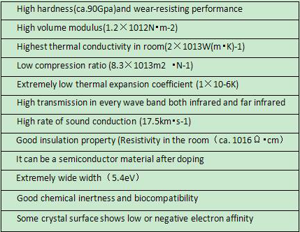
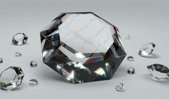
Diamond, as one of the most special materials in natural world, is featured with the highest hardness, low friction coefficient, high elasticity modulus, high thermal conductivity, high insulation class, wide energy gap, great sound propagation rate and favorable chemical stability, which are presented in below Table. In spite of such unique features, the natural diamond has always been existed in the form of gem, with its variability and rareness sharply limiting its application. Luoyang Yuxin Diamond Co., Ltd‘s CVD Diamond film, on the other hand, integrates such physical and chemical properties, with lower cost than natural diamond and applicable to be made into various shapes, thus enjoying extensive application prospect in electronic industry, optical field and mechanical industry.
