Company tel:+86-379-63184520
Contact number:+86-15937921751
Postcode:471000
Email:info@yuxindiamond.com
Address:3-1-508 Luoyang National University Science Park, No. 2 Penglai Road, Jianxi District, Luoyang, China 471000
Prototype Nuclear Battery Packs 10 times More Power
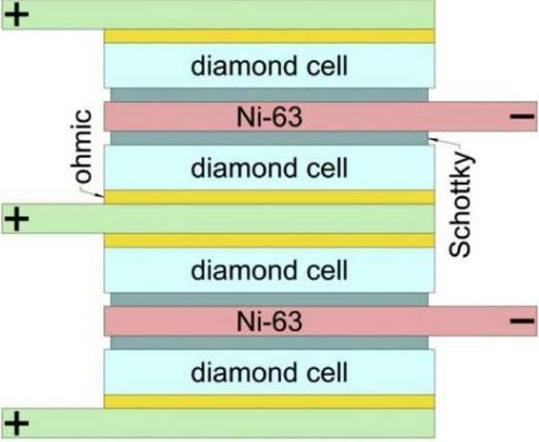
The nuclear battery prototype consisted of 200 diamond converters interlaid with nickel-63 and stable nickel foil layers (figure 1). The amount of power generated by the converter depends on the thickness of the nickel foil and the converter itself, because both affect how many beta particles are absorbed. Currently available prototypes of nuclear batteries are poorly optimized, since they have excessive volume. If the beta radiation source is too thick, the electrons it emits cannot escape it. This effect is known as self-absorption. However, as the source is made thinner, the number of atoms undergoing beta decay per unit time is proportionally reduced. Similar reasoning applies to the thickness of the converter.
The goal of the researchers was to maximize the power density of their nickel-63 battery. To do this, they numerically simulated the passage of electrons through the beta source and the converters. It turned out that the nickel-63 source is at its most effective when it is 2 micrometers thick, and the optimal thickness of the converter based on Schottky barrier diamond diodes is around 10 micrometers.
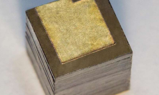
Manufacturing technology
The main technological challenge was the fabrication of a large number of diamond conversion cells with complex internal structure. Each converter was merely tens of micrometers thick, like a plastic bag in a supermarket. Conventional mechanical and ionic techniques of diamond thinning were not suitable for this task. The researchers from TISNCM and MIPT developed a unique technology for synthesizing thin diamond plates on a diamond substrate and splitting them off to mass-produce ultrathin converters.
The team used 20 thick boron-doped diamond crystal plates as the substrate. They were grown using the temperature gradient technique under high pressure. Ion implantation was used to create a 100-nanometer-thick defective, "damaged" layer in the substrate at the depth of about 700 nanometers. A boron-doped diamond film 15 micrometers thick was grown on top of this layer using chemical vapor deposition. The substrate then underwent high-temperature annealing to induce graphitization of the buried defective layer and recover the top diamond layer. Electrochemical etching was used to remove the damaged layer. Following the separation of the defective layer by etching, the semi-finished converter was fitted with ohmic and Schottky contacts.
All converters were connected in parallel in a stack as shown in figure 1. The technology for rolling 2-micrometer-thick nickel foil was developed at the Research Institute and Scientific Industrial Association LUCH. The battery was sealed with epoxy.
The prototype battery is characterized by the current-voltage curve shown in figure 3a. The open-circuit voltage and the short-circuit current are 1.02 volts and 1.27 microamperes, respectively. The maximum output power of 0.93 microwatts is obtained at 0.92 volts. This power output corresponds to a specific power of about 3,300 milliwatt-hours per gramm, which is 10 times more than in commercial chemical cells or the previous nickel-63 nuclear battery designed at TISNCM.
Nuclear batteries: Prospects
The work reported in this story has prospects for medical applications. Most state-of-the-art cardiac pacemakers are over 10 cubic centimeters in size and require about 10 microwatts of power. This means that the new nuclear battery could be used to power these devices without any significant changes to their design and size. "Perpetual pacemakers" whose batteries need not be replaced or serviced would improve the quality of life of patients.
The space industry would also greatly benefit from compact nuclear batteries. In particular, there is a demand for autonomous wireless external sensors and memory chips with integrated power supply systems for spacecraft. Diamond is one of the most radiation-proof semiconductors. Since it also has a large bandgap, it can operate in a wide range of temperatures, making it the ideal material for nuclear batteries powering spacecraft.
The researchers are planning to continue their work on nuclear batteries. They have identified several lines of inquiry that should be pursued. Firstly, enriching nickel-63 in the radiation source would proportionally increase battery power. Secondly, developing a diamond p-i-n structure with a controlled doping profile would boost voltage and therefore could increase the power output of the battery at least by a factor of three. Thirdly, enhancing the surface area of the converter would increase the number of nickel-63 atoms on each converter.
TISNCM Director Vladimir Blank, who is also chair of nanostructure physics and chemistry at MIPT, commented on the study: "The results so far are already quite remarkable and can be applied in medicine and space technology, but we are planning to do more. In the recent years, our institute has been rather successful in the synthesis of high-quality doped diamonds, particularly those with n-type conductivity. This will allow us to make the transition from Schottky barriers to p-i-n structures and thus achieve three times greater battery power. The higher the power density of the device, the more applications it will have. We have decent capabilities for high-quality diamond synthesis, so we are planning to utilize the unique properties of this material for creating new radiation-proof electronic components and designing novel electronic and optical devices."
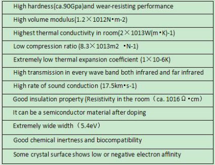
Diamond, as one of the most special materials in natural world, is featured with the highest hardness, low friction coefficient, high elasticity modulus, high thermal conductivity, high insulation class, wide energy gap, great sound propagation rate and favorable chemical stability, which are presented in below Table. In spite of such unique features, the natural diamond has always been existed in the form of gem, with its variability and rareness sharply limiting its application. Luoyang Yuxin Diamond Co., Ltd‘s CVD Diamond film, on the other hand, integrates such physical and chemical properties, with lower cost than natural diamond and applicable to be made into various shapes, thus enjoying extensive application prospect in electronic industry, optical field and mechanical industry.
