Company tel:+86-379-63184520
Contact number:+86-15937921751
Postcode:471000
Email:info@yuxindiamond.com
Address:3-1-508 Luoyang National University Science Park, No. 2 Penglai Road, Jianxi District, Luoyang, China 471000
New Insight into Nanopatterning Diamond
The ability to etch nanostructures onto the surface of diamond is expected to have a wide variety of potential applications, but so far etching and patterning diamond at the nanoscale has been challenging, as diamond is highly chemically inert (unreactive). In a new study, researchers have investigated a technique in which an electron beam is used for nanopatterning diamond, with the results offering new insight into emerging nanofabrication processes.

The researchers, James Bishop et al., at the University of Technology Sydney in Sydney, Australia, have published a paper on the nanopatterning and etching of diamond in a recent issue of ACS Nano.
In their work, the researchers investigated a technique called gas-mediated electron beam-induced etching. The method requires no mask or resist layer and uses electron beam irradiation in the presence of reactive gases to directly etch diamond and other materials with a spatial resolution as high as 10 nanometers. It also avoids the residual damage issues associated with physical etch techniques such as focused ion beam or reactive ion etching, enabling etching with minimal damage to the underlying material.
So far, most work using this method has demonstrated etching that appears uniform, or isotropic. However, in order to create desired patterns or selectively expose certain crystal planes, it becomes necessary to etch selectively in different orientations, which is called anisotropic etching.
Using a combination of experimental and computational techniques, the researchers found that oxygen and hydrogen gases play different roles in the etching process. In particular, oxygen causes rapid, efficient and isotropic etching, while the addition of hydrogen slows down the rate of etching of certain crystal planes more than others, enabling anisotropic etching. Anisotropic etching has long been used with other materials such as silicon and gallium nitride in order to create micro/nano-structures with near perfect symmetry and ultra-smooth crystal planes. This new work highlights a method to potentially achieve similar results with diamond.
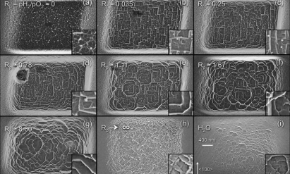
The researchers found that, as more hydrogen gas is added to the system, patterns emerge whose features are aligned with the crystal directions of the diamond lattice. The scientists explain that these patterns are caused by hydrogen's preferential passivation of certain crystal planes over others. The researchers also showed that it's possible to control the anisotropy by controlling the amount of hydrogen, and consequently, to manipulate the geometries of the surface patterns. This enabled the researchers to create a detailed model of the etch kinetics, which should simplify future dry etch nanofabrication processes for diamond and enable fabrication of previously untenable structures.
"The most significant outcome of the work is the control over etch anisotropy that it enables," Bishop told Phys.org. "Isotopic etching is useful for etching arbitrarily shaped structures. Anisotropic etching is useful for creating structures with ultra-smooth surfaces and near-perfect symmetries defined by the kinetics of the anisotropic etch reaction. With electron beam-induced etching using oxygen we can obtain high rate isotropic etching, and by mixing in hydrogen, achieve highly anisotropic etching of diamond."
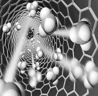
The ability to controllably etch nanopatterns and selectively expose and smooth certain crystal planes on the surface of diamond has a wide variety of potential applications. Different nanopatterns and nanostructures can, for example, expedite neuron growth on diamond surfaces for biosensing applications, as well as enhance light extraction for photonic applications. Diamond is also being investigated for its possible applications for high-power electronics, electrochemistry, and catalysis, all of which may benefit from a simple, high-resolution nanopatterning method.
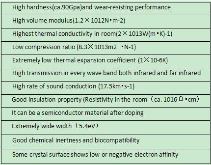
Diamond, as one of the most special materials in natural world, is featured with the highest hardness, low friction coefficient, high elasticity modulus, high thermal conductivity, high insulation class, wide energy gap, great sound propagation rate and favorable chemical stability, which are presented in below Table. In spite of such unique features, the natural diamond has always been existed in the form of gem, with its variability and rareness sharply limiting its application. Luoyang Yuxin Diamond Co., Ltd‘s CVD Diamond film, on the other hand, integrates such physical and chemical properties, with lower cost than natural diamond and applicable to be made into various shapes, thus enjoying extensive application prospect in electronic industry, optical field and mechanical industry.
