Company tel:+86-379-63184520
Contact number:+86-15937921751
Postcode:471000
Email:info@yuxindiamond.com
Address:3-1-508 Luoyang National University Science Park, No. 2 Penglai Road, Jianxi District, Luoyang, China 471000
Forming and sensing optical emitters in real time
by Kat J. McAlpine, Harvard John A. Paulson School of Engineering and Applied Sciences

Credit: Harvard John A. Paulson School of Engineering and Applied Sciences
Seeking new techniques to enable quantum networking, Harvard University researchers have developed a novel laser-based strategy for creating single-atom, near-surface material defects, which can be used to form qubits, the most fundamental units of quantum computing. The team also discovered a real-time method for measuring and characterizing the formation of optical emitters within nanoscale cavities.
The advance, reported in Nature Materials by Evelyn Hu and her team at the Harvard John A. Paulson School of Engineering and Applied Sciences (SEAS), could enable better control over the timing and strength of qubit outputs.
"These are essentially 'defective' materials; there's an absence of an atom, or a vacancy, in an otherwise perfect crystal structure," says Hu, senior author on the paper and the Tarr-Coyne Professor of Applied Physics and of Electrical Engineering at SEAS. "A vacancy has its own electronic states, it has a certain spin, and it has the potential to emit photons of a particular wavelength."
These defects and the wavelengths of light they emit are sometimes called color centers because they can give diamonds and other crystals beautiful colors. But inside a nanoscale cavity in a photonic material—which refract, control, or manipulate light—these defects can act like optical emitters of information.
"Our team is really interested in the formation of these defects and how they could behave as qubits in a quantum network. Coupling an array of defects in nanophotonic cavities via entanglement would allow transmission of quantum information," says Aaron Day, a co-first author of the paper. He and the paper's other co-first author, Jonathan Dietz, are both applied physics Ph.D. candidates in Hu's lab.

Image by LifetimeStock/Shutterstock
Yet until now, there has been no way to totally control the exact location of optical emitters in nanoscale cavities without damaging the rest of the material's crystal structure.
Typically, the process to create emitters within cavities like this—100x smaller than the width of a human hair—requires disrupting a material's crystal structure using ions or below-band-gap lasers. (Band gap refers to the minimum amount of energy required to excite a material's electrons so that they can freely conduct current.) But ion implantation equipment isn't available in most labs. And Hu says both conventional techniques are "brute-force" uses of kinetic energy that are inefficient and difficult to control—more like sandblasting than careful drilling.
"To do what we wanted to do, we knew we needed to develop some extremely precise instruments," Hu says.
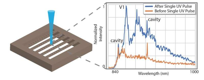
The team likens their solution to a stylus and template, using a laser (the stylus doing the writing) and a cavity (the template into which one writes) to form and characterize the vacancy formation. "We wanted to do this using above-band-gap pulses of light"—containing more photon energy than below-band-gap lasers—"to more efficiently transfer energy from the laser 'stylus' to the material 'template,'" Day says.
First, Day and Dietz fabricated nanophotonic cavity devices out of commercial-grade silicon carbide in a clean room, a time-consuming and painstaking endeavor. Then they ran experiments to attempt creating optical emitters exactly where they wanted inside the cavities.
"At first, our laser pulses were blowing up our cavities—exploding them, basically," Day says, an outcome that was far from ideal. "We needed to reduce the energy of the laser dramatically."
Through trial and error, they determined how much energy and how much energy was needed to create the desired emitter while preserving the rest of the cavity without causing a "blow up." They also built into their system an additional "read-out" laser, enabling them to assess the resonance, or photonic signals, given off by a cavity before and after it was pulsed by the defect-forming laser.
"One of the coolest things we found is that we could monitor the cavity, do one laser pulse to create the optical emitter, and then get a read-out of immediate changes to the cavity," Day says.
"The most exciting potential of our work is in creating scalable numbers of qubits. A means of creating and assessing emitters in real-time makes it much easier to pick a cavity with the right properties and reliably turn it into a host for quantum information," says Dietz.
Moreover, Hu's team says their approach could be broadly useful for a range of fundamental questions.
"As we form defects within cavities, we can use those cavities to instantly tell us information about the local material environment—using it as a 'nanoscope' to probe the characteristics of atomic defects," Day adds. "Combining this new laser stylus with the template of using cavity resonances to provide us with real-time feedback allows us to write and improve devices seamlessly. These two tools, together, are more powerful than either of them would be on their own."


